I remember this is
my first design during my undergraduate studies in
Universiti Teknologi Malaysia (UTM) in 2004. On this entry, i would like
to share with you how i come out a core or engine or some people say IP design.
It looks simple, but it show the fundamental how we should apply some law in
design our circuits using HDL.
Lets talks about the
design. Here Greatest Common Divisor (GCD) is going to design using
Verilog.
The GCD
calculator to be designed has the following specifications:
It
computes the greatest common divisor (gcd) of a pair of 8-bit binary positive
numbers. The operand registers are initialized with the activation of a start signal,
which commences the computation process. Once the operation completed, a signal valid is
asserted to indicate that the data on the gcd outputs are valid.
Algorithmic modeling:
In this step , the specifications are translated to produce
the behavioral model of the gcd
calculator. This model can be expressed in terms of an algorithm as shown below.
- INITIALIZE
- IF p>q THEN
p=p-q
ELSE IF p<q THEN
q=q-p
ELSE gcd=p
- END
Meanwhile the flowchart for this design shows in Figure 1.

Figure 1: Flowchart of GCD Calculator
RTL Modelling:
The behavioural model is now refined to obtain an equivalent
RTL model. This model can be the form of an ASM flowchart as shown in Figure 1.
From this ASM flowchart, the following RTL Code is derived:

In bold fonts,
the RTL statements correspond to data operations: while the statements in italic fonts correspond to control
operations.
RTL Design:
Construct the functional block diagram of the datapath unit
and annotate all the control signals in the diagram. This is shown in figure 2.

Figure 2: Functional Block Diagram of Data Path Unit GCD Calculator
Then I construct the RTL Control State table is obtained as
in Figure 3.

Figure 3: RTL-CS Table for GCD Calculator
The block diagram of Control Unit GCD Calculator is shown in
figure 4.

HDL coding of the RTL
design
From the functional block diagram in Figure 2, the HDL codes
of Datapath GCD calculator is now
generated as shown in figure 5 below.

Figure 5: Verilog
Code of Data path GCD Calculator
From the functional block diagram in Figure 3 and Figure 4,
the HDL codes of Control Unit GCD
calculator is now generated as shown in figure 6 below.

Figure 6: Verilog Code of Control unit GCD Calculator
Derive the HDL coding for the top-level module by
integrating this Datapath (Figure5) and Control_Unit (Figure 6) into a main
module by apply structural modeling style as shown in figure 7.

Figure 7: Top-level input output block diagram of GCD Calculator
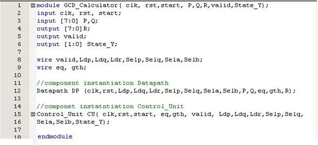
Figure 8: Verilog
code of GCD Calculator Design
Simulation
In order to verify functionality of this design, I need use
waveform simulation. For example, to test GCD between number 2 and 8, the
result should be 2 as shown in Figure 9.

Figure 9: Waveform Simulation for GCD 2 and 8.
Now you can test a few test vector by setting a value in
inputs P and Q. Observe the output R once signal valid activated.
Have a nice day!
how to wright test bench?
ReplyDeleteAssalaamu alaikum, I have some questions can you email your email ID to zakirhussainwork@gmail.com
ReplyDeleteYou design based subtraction loop, today most of the FPGA's contain Embedded Multiplier. It should reduce calculation time
ReplyDeleteFriend
This comment has been removed by the author.
ReplyDelete