This tutorial requires the following hardware and software:
1. A PC running the XP operating systems.
2. QuartusII sotware version 7.2 sp3.
3. NiosII EDS version 7.2 sp3.
4. MegaCore IP Library version 7.2 sp3.
5. A Cyclone II DE2 NiosII Develepmont Board.
This tutorial assumes that you are familiar with Quartus II software, Nios II Development Board device and peripherals, NiosII SOPC Builder and fundamental of C programming.
Quadratic equation
In mathematics, a quadratic equation is a polynomial equation of the second degree. The general form is

where x represents a variable, and a, b, and c, constants, with a ≠ 0. (If a = 0, the equation becomes a linear equation.) The constants a, b, and c, are called respectively, the quadratic coefficient, the linear coefficient and the constant term or free term. The term "quadratic" comes from quadratus, which is the Latin word for "square". Quadratic equations can be solved by factoring, completing the square, graphing, Newton's method, and using the quadratic formula.
Quadratic Formula
A quadratic equation with real or complex coefficients has two solutions, called roots. These two solutions may or may not be distinct, and they may or may not be real.
The roots are given by the quadratic formula

are solutions of the quadratic equation.
Block Diagram of Quadratic Formula

Figure 1: Block Diagram of Quadratic Formula
Based on Figure 1, this quadratic formula uses 5 multipliers, an adder/subtraction, a subtraction, a square root and divider. All these components are floating point unit. In this exercise, we do not to design all these module but we will use MegaWizard LPM IP on Altera QuartusII software.
Create a new project in Quartus II
1. Open QuartusII and create a new project.
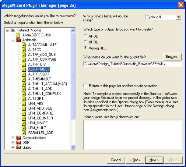
2. Click Tools-->MegaWizard Plug-In Manager to Create a new custom megafunction variation. Then click Next.

3. Select a megafunction from Arithmetic folder and select ALTFP_MULT, name it as FPMult.v. This wizard will create floating point multiplier 32-bit single precision. Click Next.
4. Remove unnecessary input/signal output for simplicity of the design.

5. Click Finish button to end this wizard. Repeat again from step 2 for module ALTFP_ADD_SUB ( floating point of adder and subtraction), ALTFP_ADD_SUB( subtraction), ALTFP_DIV (divider ), ALTFP _SQRT ( square root).
Build a Quadratic module
1. Create a new HDL file.

2. Copy the following code and paste it into a new verilog file, name it as Quadratic.v.

3. Compile Quadratic.v and observe the compilation report shows utilization resources.

Verify the Quadratic module design
- Lets say we have a simple quadratic equation , y = 4x2+2x-2 so that the actual graphs is

a = 4, b = 2, c = -2. Discriminant: b2-4ac = 2 2+4*4*(-2) = 36 . Discriminant (36) is greater than zero. The equation has two solutions.
x1,2 = 0.5, -1
These value are floating point representation, but in our quadratic module receives value in HEX number.
Floating point number Hex number (32-bit) 2 40000000 4 40800000 -2 C0000000 -1 BF800000 0.5 3F000000
2. Lets perform waveform simulation on Quadratic module based on test vector (value Hex) in the previous table.3. Create a new Vector Waveform File.
4. Verify the output waveform should appear the expected result at port x in Simulation Report.

Create User Logic Quadratic module1. Now we need to port Quadratic module into NiosII system bus, therefore a interface module that connect between Quadratic module and to Avalon Bus.2. Copy the following code and compile all modules again.

3. You can see the overall datapath, click Netlist_ViewersàRTL Viewer.
Create SOPC System1. Click ToolsàSOPC Builder to create new system.
2. Create this system that consist of SDRAM Controller, Nios II processor, JTAG, timer and User_Logic_Quadratic( rename to core). The process to integrate the User_Logic_Quadratic into NiosII system can be refer to previous tutorial/technical report.3. The SOPC system structure is shown in figure below.
4. Click Generate to complete this process. Then Exit.Compile SOPC System1. Create PLL module using MegaWizard function (pls refer previous tutorial/technical report to create PLL module) and copy the following code into a new HDL file. Name it as Top_Level.v
2. Import DE2_pin_assigment.csv before compile it.
Design the Embedded Software System1. Open NiosII IDE program to start NiosII IDE. Create a new NIOSII C/C++ Application.2. Browse the ptf file reside in your work folder. 3. Create a new Source File , name it as Quadratic.c
4. Copy and paste the following c code and save it.


5. Debug and run as NiosII Hardware. 6. Verify the functionality and observe the performance.
Observation and Conclusion- Lets benchmarked some example in the table below:
Quadratic Equation
Ax2 + Bx + C = 0 Test No Input Output A B C X1 X0 1 -5 4 3 -0.4718 1.2718 2 -53 34 87 -1 1.6415 3 0.256 0.614 -0.65 0.7951 -3.1935 4 -5 -9.6 -2.64 -1.5873 -0.3326
- Result on NiosII Console as shown in figure below.

- Result for performance
Test No No of Software ticks No of Hardware ticks Speed Gain 1 40914 22963 1.78 2 36370 32181 1.13 3 41064 11275 3.64 4 41152 25553 1.6


