A multiplexer is one of the importance or ‘must’ component
in the digital system generally. The
multiplexer is basic combinational logic circuits where it will be selects one of several input signals
and passes it on the output. The routing of the desired data input to the
output is controlled by SELECT inputs. Figure 1 show the block diagrams of 4to1
Multiplexer, where 4 inputs, 2 selectors and 1 output.
Figure 1: A Block Diagram of Multiplexer 4to1
Table 1 shows the truth table of this 4to 1 multiplexer.
Then the complete equation can be generate as
Z= ASel1Sel0 + BSel1Sel0 + CSel1Sel0 + DSel1Sel0
Table 1: Truth Table for Multiplexer
In this post, I will show you a few type of Verilog code to
represent a multiplexer especially in my tutorial here, multiplexer 4to1.
Boolean Equation based Modelling
On this modelling, the output signals are specified in terms
of input signal transformation based on Boolean equations. This modelling style
allows a digital system to be designed in terms of its function. Let’s look at
Figure 2 shows a Verilog code to implement this example of Multiplexer 4to1.
Figure 2: A Combinational Logic of Multiplexer 4to1 Verilog Code
Case Statement
The Verilog case statement is similar to its counterpart in
other languages. It searches from top to bottom to find a match between the
case expression and a case item. The case statement executes the statements
associated with the first match found, and then does not consider any remaining
possibilities. Figure 3 shows how the Multiplexer 4to1 can be write in this
case statement style.
Figure 3: A
Multiplexer based circuit using case statement
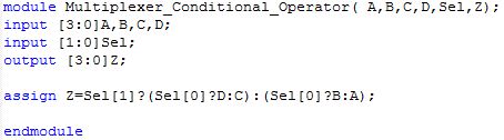
Conditional Operator
The condition expression using the conditional operator,
denoted by “?:” symbol. The expression
“ a? b:c ” read as: “
if a is true then the result of the expression is b else the result is c”
In Figure 4 shows example how implementation of Multiplexer
2to1 using this conditional operator.
Figure 4:
Modelling a Multiplexer 2to1 with conditional operator
Then if you understand behaviour in Figure 4, now you can
construct Multiplexer 4to1 using same method as shown in Figure 5a using
structural modelling and purely conditional operator in Figure 5b.
Figure 5a : Structural Modelling
Figure 5b : Conditional Operator
Now you know how to construct 8to1 Multiplexer, right?
If-then-else statement
The conditional IF statement executes a statement if a
condition is true. There are two other variants available: if-else and if-else-if statement.
Figure 6 shows the implementation of multiplexer 4to1 using
if-else-if statement.
Figure
6: A Multiplexer 4to1 using if-else-if statement
Performance
Now, come in my mind, what about the performance for each
different type of multiplexer above? Which type of style of Verilog should I
apply? I believe it could be significant performance should be found. I’m not
going to do some evaluation here, but based on RTL Viewer from QuartusII Tool
may indicate something that needs to look further.
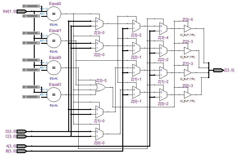
Let see in Figure 7, Figure 8, Figure 9 and Figure 10 shows
RTL Viewer for Combinational Logic, Case Statement, Conditional Operator and If-then-else
statement respectively. Probably you may some idea. Please post your comment
regarding on this issue. Thank you again.
Figure 7: RTL Viewer for Multiplexer 4to1 for Combinational
Logic
Figure 8: RTL Viewer for Multiplexer 4to1 for Case Statement
Figure 9: RTL Viewer for Multiplexer 4to1 for Conditional Operator
Figure 10: RTL Viewer for Multiplexer 4to1 for If-then-else statement