On this tutorial, we would like to use one of the LPM Megawizard components in Quartus II and test it the functionality through Nios II processor. We are going to use a 32-bit single precision floating point adder as our reference design.
In this tutorial, the following example is based on :
- Quartus II ver 7.2
- NiosII 7.2 IDE
- DE2 cycloneII development board, USB Blaster
- XP Operation System
Create Floating Point Adder from Altera MegaWizard LPM
1. Open Quartus II software. Create a new Quartus II project .
2. Click àMegaWizard Plug-In Manager to create a new custom megafunction variation.
3. Select a megafunction ALTFP_ADD_SUB in Arithmetic folder. Then name it as FloatingPoint.v. Click Next.
4. Follow these setting for this tutorial. Finally click Finish button.
5. In this tutorial we would like to have rdy signal in this floating point adder module. So create a new verilog file and copy this following code. Name it as FloatingPointCore.v .This signal rdy will active when the counter (cont) reach 14 clock cyle.
6. Save and run the design.
Design User Logic Floating Point
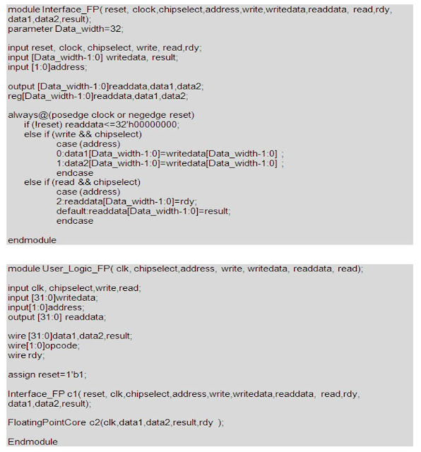
- Now we need to create a module that interface with NiosII bus system. The block diagram of this design as shown in following figure.
2. Now copy Interfece_FP.v and User_Logic_FP.v into your project. Save and run.
Integrate Peripherals into NIOS II System Module
1. Go to ToolsàSOPC Builder to open a Create A New System. Perform the followings seeting: System Name: Sopc_system. Target HDL: Verilog.
2. In Clock Settting: Name clk, Source-External, Mhz-100.Mhz
3. Adding Memories and Memory ControlleràSDRAMàSDRAM Controller.
4. Select Nios II Processor.
5. Add JTAG UART from Interface ProtocolsàSerial.
Integrate User_Logic_FP into NIOS II System Module
1. Double click Create New Component and then Component Editor will displays.
2. Select HDL Files then, click Set HDL Files. Browse to the User_Logic_FP.v.
3. Select signal tab and verify that should same as the following figure.
4. Select Interface tab. Change wait state for read and write operation is set to 1.
5. Click Finish button. Now Observe SOPC Builder Component , you can see a new library called User_Logic_FP. Now double click on User_Logic_FP to add this design into NIOS II System Module. Click Finish. Rename to core.
6. Click SystemàAuto-Assign Base Address. Then click Generate button.
7. After generation is completed. Click Exit.
Create the PLL component.
1. Click ToolsàMegaWizard Plug-In Manager to create PLL.v. Follow the guide as per following picture.
2. Then click Finish button.
Compile the top level design.
1. Create the top level design, Top_Level.v, which is consist of Sopc_system and PLL components.
2. Click AssignmentàImport Assignment. Select DE_2_pin_assignment.csv.
3. Save and Compile the entire design. Make sure Top-level entity is set to Top_Level before compile it.
Design the Embedded Software.
1. Open NiosII 7.2 IDE. From FileàNewàNiosII C/C++ Application.
2. Specify the following options
3. Click Finish. Right click Floating_Point_Adder, click New then Source File to create new source file (.c).
4. Copy this following code.
5. Save it as main.c
6. Right click the Floating_Point_Adder project in the NIOSII C/C++ project view and click Build project.
Download Hardware Design into FPGA.
- Congratulation!


No comments:
Post a Comment